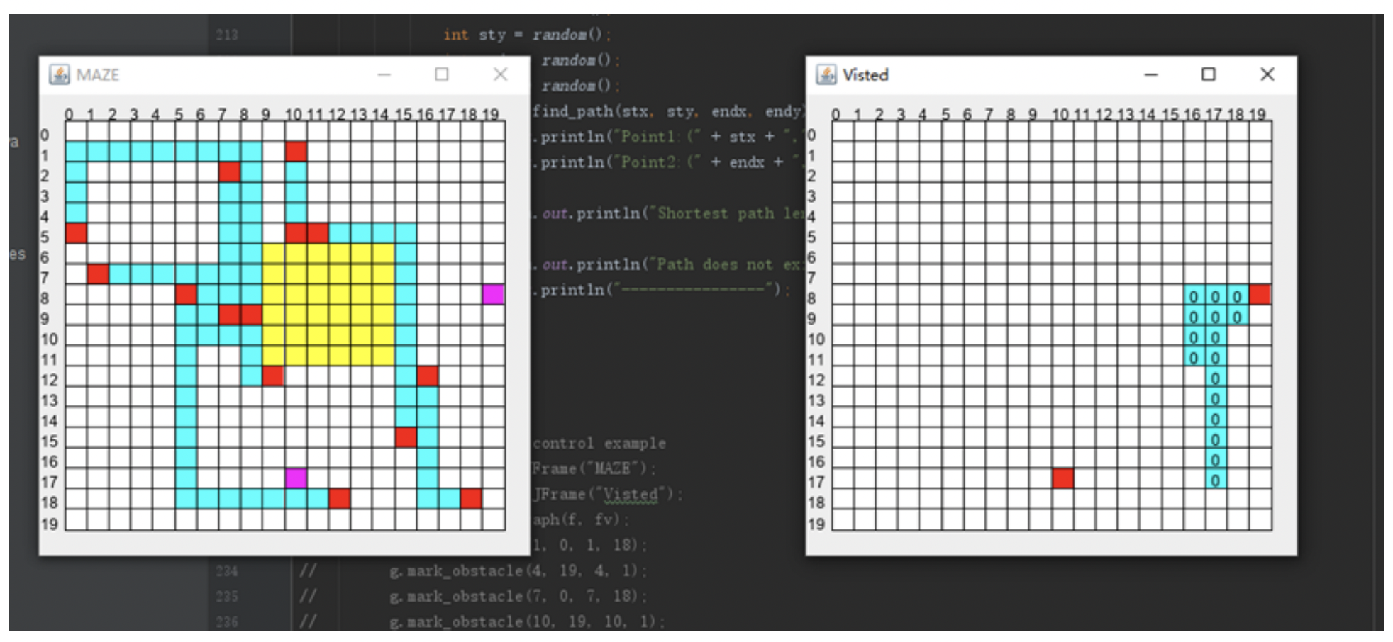
Solving Printed Circuit Board Routing Problem Using Lee’s and Hadlock’s Maze Routing Algorithm

Abstract
Wire routing is one of the major steps in designing printed circuit board (PCB). In a one-layer PCB design, the target is to implement circuit wires by placing terminals and connecting them with conductive metal traces on a plane, under the restriction that latterly added wires should not intersect existing ones. Under the assumption of fixed trace width, we formulated this problem as a maze routing problem, i.e., finding paths that connect pairs of square cells in a grid, while avoiding cells marked as obstacles. We implemented the Lee’s algorithm and the Hadlock’s algorithm to solve this problem, and discussed the differences in time complexity between the two algorithms.